Monolithic neural silicon bonded directly to atomic-layer ceramic substrates. Eliminating interconnect latency for next-generation exascale intelligence.
Class-10 metallization with sub-micron line pitches. 1.8 TB/s bi-directional die-to-die bandwidth with near-zero parasitic capacitance.
Engineered with direct thermal copper vias and vapor chambers to sustain continuous 400A loads across high-concurrency matrix calculations without thermal throttling.
Standard FR4 PCB materials collapse under the extreme dielectric losses of multi-gigahertz optical and neuromorphic interconnects. Valence utilizes proprietary alumina-zirconia ceramic substrates with isotropic coefficient of thermal expansion matching single-crystal silicon.
Direct copper and gold sputter deposition achieving 99.999% purity and sub-surface roughness under 25 nm.
Loss tangent tan δ = 0.0004 at 112 GHz PAM4 signaling, reducing signal degradation by 74% over Teflon substrates.
Continuous solid-copper thermal conduits conducting 380 W/(m·K) straight from the die micro-bumps to carrier heatsinks.
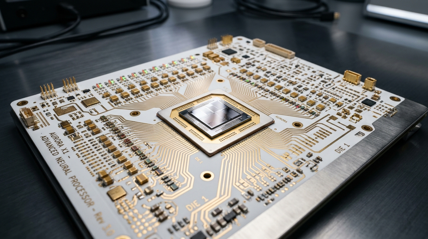
Integrated GaN power converters sitting directly under the die cavity to eliminate dI/dt voltage drop under sudden computational spikes.
Direct laser diode alignment trenches etched onto the substrate edges for 3.2 Tbps optical wavelength multiplexing.
Inspect the physical sub-blocks of the Aurora X1 accelerator. Switch between die layers to view telemetry, bandwidth parameters, and silicon floorplan allocation.
Consists of 256 independent systolic processing arrays optimized for transformer attention mechanisms and sparse matrix dot-products with dynamic sparsity gating.
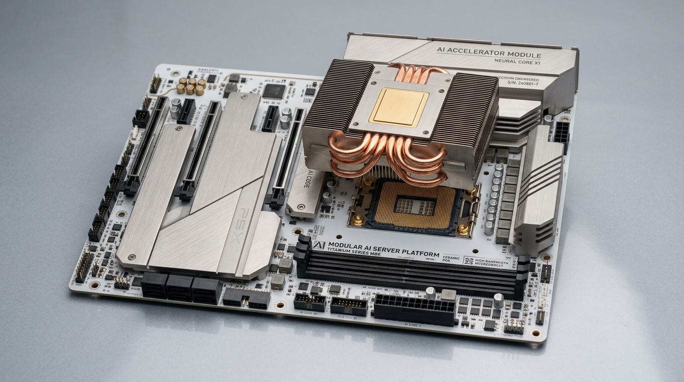
Engineered for hyperscale datacenter deployments. The Titanium MBX platform features hot-swappable accelerator sockets, CXL 3.1 memory pooling, and ultra-flat vapor-chamber thermal dissipation.
Direct-contact sintered copper micro-heatpipes coupled with precision milled aluminum cooling fins capable of dissipating up to 600W sustained thermal load.
4,896 beryllium-copper contacts with 30µ-inch gold plating, providing redundant power ground planes and 128 differential high-speed PCIe 6.0 lanes.
Native hardware coherence allowing up to 16 accelerator boards to share a unified 2 Terabyte memory pool over low-latency optical links.
Complete electrical, thermal, and mechanical parameters for the Aurora X1 silicon die and Titanium ceramic carrier boards.
| Domain / Parameter | Aurora X1 Monolithic Die | Titanium MBX Motherboard | Test Conditions & Compliance |
|---|---|---|---|
| Process Node / Substrate | 3nm FinFET / High-k Metal Gate | 28-Layer Al2O3-Zr Ceramic HDI | Class 10 Cleanroom fab |
| Compute Throughput | 1,024 TFLOPS (FP8 Sparse) | Up to 8x Sockets (8,192 TFLOPS) | Dense GEMM @ 2.45 GHz |
| Interconnect Bandwidth | 1.8 TB/s Die-to-Die Fabric | 3.2 Tbps Silicon Photonics C-Band | 112 Gbps PAM4 / BER < 10⁻¹⁸ |
| Memory Subsystem | 96 GB HBM3e Co-Packaged | 512 GB DDR5-6400 ECC Registered | 4.8 TB/s Peak HBM Throughput |
| Power Delivery & Envelope | 350W TDP Nominal (0.75V - 1.1V) | 48V to 12V Direct Bus / 400A VRM | Sub-nanosecond dI/dt response |
| Thermal Resistance (θjc) | 0.03 °C/W (Gallium-Indium TIM) | Vapor Chamber + Micro-Finned Sink | Liquid loop delta < 15°C |
| Form Factor & Mounting | 32.5 × 24.0 mm Bare Die Interposer | Standard Open Compute Project (OCP 3.0) | EIA-310 1U/2U Rack Mount |
Valence provides direct engineering access for custom ASIC interposer layout, multi-project wafer (MPW) shuttle slots, and reference evaluation boards.