AURORA X1 ARCHITECTURE // REV 3.0
[ 01 // PHYSICAL FOUNDATION ]

The Architecture of Pure Conduction.

Monolithic neural silicon bonded directly to atomic-layer ceramic substrates. Eliminating interconnect latency for next-generation exascale intelligence.

[ 02 // SUB-MICRON INTERCONNECT ]

Ultra-Dense Gold & Copper Topologies.

Class-10 metallization with sub-micron line pitches. 1.8 TB/s bi-directional die-to-die bandwidth with near-zero parasitic capacitance.

0.8 µm Trace Pitch
< 0.12 ps Propagation Skew
[ 03 // THERMAL EQUILIBRIUM ]

Cryogenic Precision. Unbounded Throughput.

Engineered with direct thermal copper vias and vapor chambers to sustain continuous 400A loads across high-concurrency matrix calculations without thermal throttling.

Scroll to Explore Die Metrology
01 // Material Science

Ceramic Matrix & High-Density Interconnects.

Standard FR4 PCB materials collapse under the extreme dielectric losses of multi-gigahertz optical and neuromorphic interconnects. Valence utilizes proprietary alumina-zirconia ceramic substrates with isotropic coefficient of thermal expansion matching single-crystal silicon.

Atomic-Layer Trace Metallization

Direct copper and gold sputter deposition achieving 99.999% purity and sub-surface roughness under 25 nm.

Isotropic Dielectric Loss Tangent

Loss tangent tan δ = 0.0004 at 112 GHz PAM4 signaling, reducing signal degradation by 74% over Teflon substrates.

Integrated Thermal Copper Pillars

Continuous solid-copper thermal conduits conducting 380 W/(m·K) straight from the die micro-bumps to carrier heatsinks.
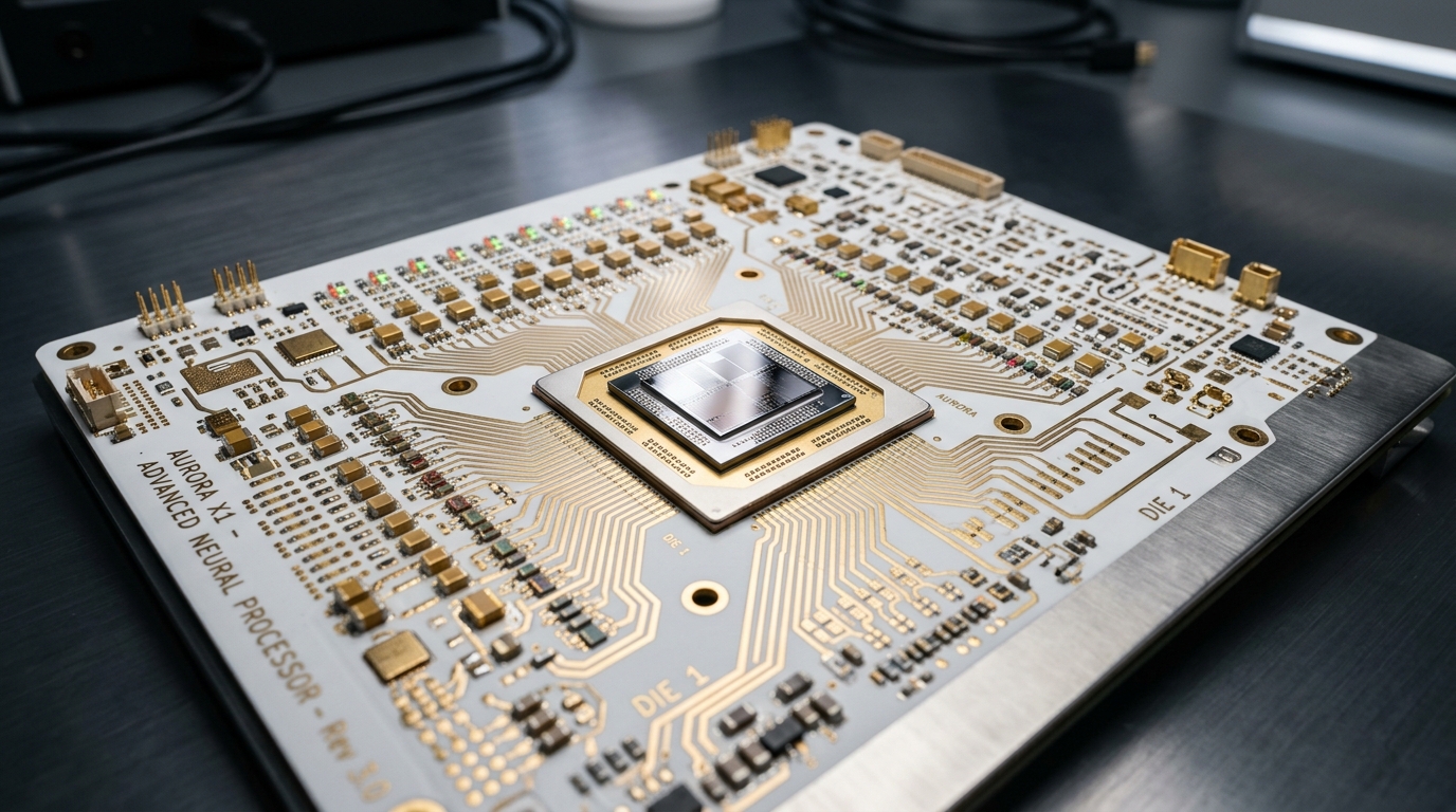
Valence Aurora X1 Ceramic Motherboard
Substrate Specification

Valence Gen-3 Al2O3-Zr High-Frequency Motherboard

Layers 28 HDI Stack
Die Gap 12.5 µm Bump
CTE Mismatch < 0.15 ppm/K
Sub-Nanosecond VRM

Embedded Power Stages

Integrated GaN power converters sitting directly under the die cavity to eliminate dI/dt voltage drop under sudden computational spikes.

Zero-Contact Optical

Photonic Micro-Interposer

Direct laser diode alignment trenches etched onto the substrate edges for 3.2 Tbps optical wavelength multiplexing.
02 // Silicon Metrology

Aurora Bare Silicon Die Matrix.

Inspect the physical sub-blocks of the Aurora X1 accelerator. Switch between die layers to view telemetry, bandwidth parameters, and silicon floorplan allocation.

LAYER 01: NEURAL TENSOR ARRAY
TSMN-912 // 3nm MONOLITHIC
Select Die Micro-Architecture Layer:

Aurora Tensor Engine Micro-Floorplan

Consists of 256 independent systolic processing arrays optimized for transformer attention mechanisms and sparse matrix dot-products with dynamic sparsity gating.

Clock 2.45 GHz
TDP 280 W
Die Size 780 mm²
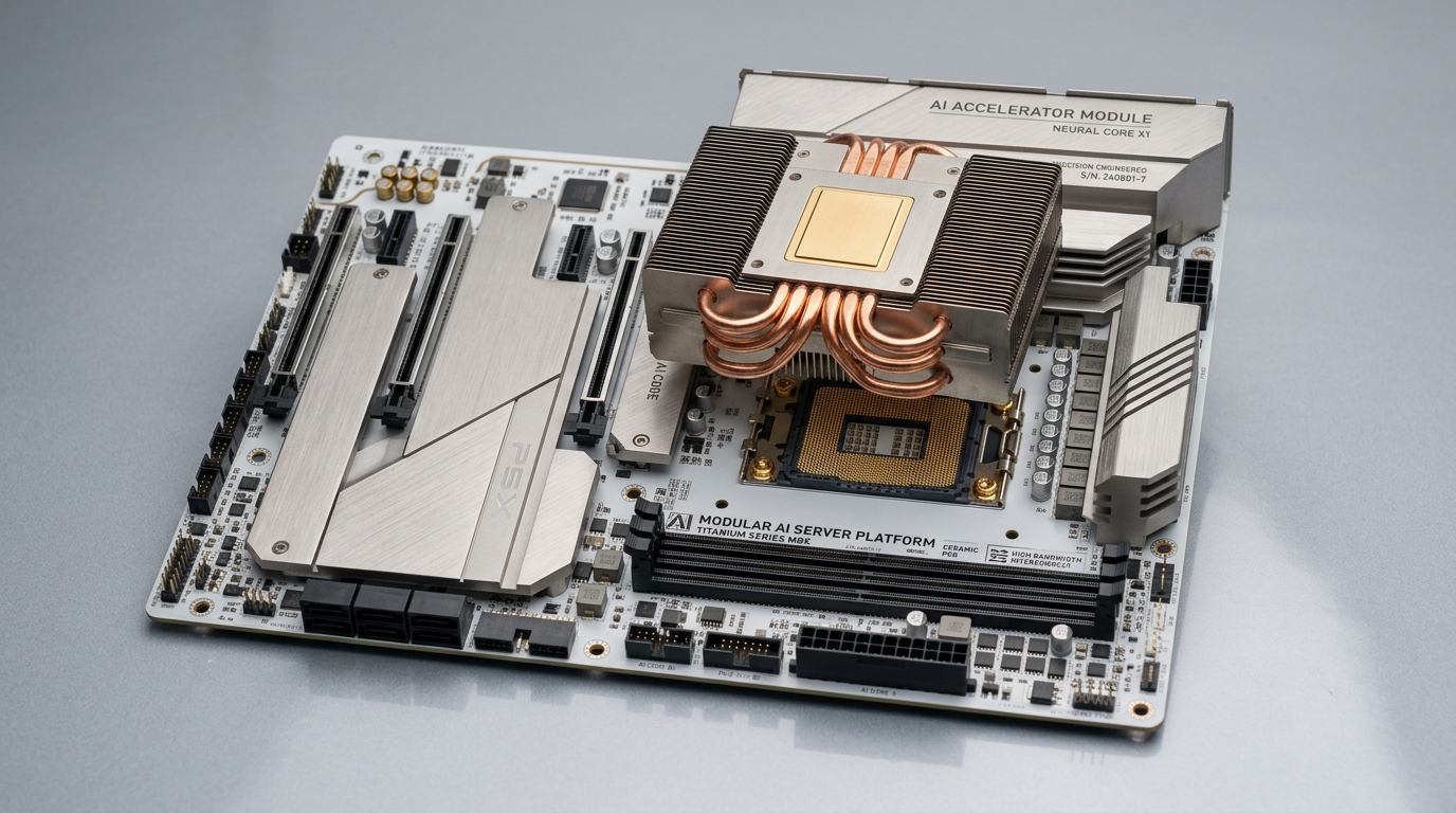
Modular AI Accelerator Server Platform
TITANIUM SERIES MBX // HIGH-BANDWIDTH FABRIC
03 // Platform Topology

Modular AI Accelerator Motherboard.

Engineered for hyperscale datacenter deployments. The Titanium MBX platform features hot-swappable accelerator sockets, CXL 3.1 memory pooling, and ultra-flat vapor-chamber thermal dissipation.

Dual-Tier Vapor Chamber Cooling

Direct-contact sintered copper micro-heatpipes coupled with precision milled aluminum cooling fins capable of dissipating up to 600W sustained thermal load.

LGA-4896 Gold Socket Matrix

4,896 beryllium-copper contacts with 30µ-inch gold plating, providing redundant power ground planes and 128 differential high-speed PCIe 6.0 lanes.

CXL 3.1 Disaggregated Memory Fabric

Native hardware coherence allowing up to 16 accelerator boards to share a unified 2 Terabyte memory pool over low-latency optical links.

04 // Verification & Parameters

Engineering Specifications Matrix.

Complete electrical, thermal, and mechanical parameters for the Aurora X1 silicon die and Titanium ceramic carrier boards.

Domain / Parameter Aurora X1 Monolithic Die Titanium MBX Motherboard Test Conditions & Compliance
Process Node / Substrate 3nm FinFET / High-k Metal Gate 28-Layer Al2O3-Zr Ceramic HDI Class 10 Cleanroom fab
Compute Throughput 1,024 TFLOPS (FP8 Sparse) Up to 8x Sockets (8,192 TFLOPS) Dense GEMM @ 2.45 GHz
Interconnect Bandwidth 1.8 TB/s Die-to-Die Fabric 3.2 Tbps Silicon Photonics C-Band 112 Gbps PAM4 / BER < 10⁻¹⁸
Memory Subsystem 96 GB HBM3e Co-Packaged 512 GB DDR5-6400 ECC Registered 4.8 TB/s Peak HBM Throughput
Power Delivery & Envelope 350W TDP Nominal (0.75V - 1.1V) 48V to 12V Direct Bus / 400A VRM Sub-nanosecond dI/dt response
Thermal Resistance (θjc) 0.03 °C/W (Gallium-Indium TIM) Vapor Chamber + Micro-Finned Sink Liquid loop delta < 15°C
Form Factor & Mounting 32.5 × 24.0 mm Bare Die Interposer Standard Open Compute Project (OCP 3.0) EIA-310 1U/2U Rack Mount
05 // Tapeout & Sampling

Request Silicon Samples & Custom Substrate Runs.

Valence provides direct engineering access for custom ASIC interposer layout, multi-project wafer (MPW) shuttle slots, and reference evaluation boards.

Q3 Tapeout Shuttle: Open for Design Submissions
Lead Time: 14 Weeks from GDSII Sign-off
AS9100D & ISO 9001:2015 Certified Cleanrooms